
Author Affiliations
Abstract
1 School of Materials Science and Engineering, Shanghai University, Shanghai 200444, China
2 Nanofabrication Facility, Suzhou Institute of Nano-Tech and Nano-Bionics, Chinese Academy of Sciences, Suzhou 215123, China
3 School of Nano-Tech and Nano-Bionics, University of Science and Technology of China, Hefei 230026, China
This letter showcases the successful fabrication of an enhancement-mode (E-mode) buried p-channel GaN field-effect-transistor on a standard p-GaN/AlGaN/GaN-on-Si power HEMT substrate. The transistor exhibits a threshold voltage (VTH) of ?3.8 V, a maximum ON-state current (ION) of 1.12 mA/mm, and an impressive ION/IOFF ratio of 107. To achieve these remarkable results, an H plasma treatment was strategically applied to the gated p-GaN region, where a relatively thick GaN layer (i.e., 70 nm) was kept intact without aggressive gate recess. Through this treatment, the top portion of the GaN layer was converted to be hole-free, leaving only the bottom portion p-type and spatially separated from the etched GaN surface and gate-oxide/GaN interface. This approach allows for E-mode operation while retaining high-quality p-channel characteristics.
GaN pFET E-mode H plasma treatment ION/IOFF ratio Journal of Semiconductors
2023, 44(11): 112801
1 北京工业大学信息学部 光电子技术教育部重点实验室,北京 100124
2 长春理工大学 高功率半导体激光国家重点实验室,吉林 长春 130022
3 中国科学院 苏州纳米技术与纳米仿生研究所,江苏 苏州 215123
采用脉冲直流磁控溅射法在Si(100)衬底上制备了AlN/Mo/Sc0.2Al0.8N复合结构薄膜,在该结构上通过金属有机化学气相沉积(MOCVD)技术进行GaN薄膜的外延。使用原子力显微镜、高分辨X射线衍射、粉末X射线衍射、扫描电子显微镜和拉曼光谱研究了Mo插入层的厚度对Sc0.2Al0.8N缓冲层和GaN外延层晶体质量的影响,研究了Sc0.2Al0.8N缓冲层对Mo上生长的GaN外延层的影响。研究结果表明,Mo插入层的厚度是影响Sc0.2Al0.8N缓冲层和GaN外延层的重要因素,Sc0.2Al0.8N缓冲层对Mo上GaN晶体质量的提高具有重要意义。随Mo厚度的增加,Sc0.2Al0.8N缓冲层的表面粗糙度先减小后增大,GaN外延层的(002)面X射线衍射摇摆曲线半峰全宽先减小后增大。当Mo插入层厚度为400 nm时,GaN外延层的晶体质量最好,GaN(002)面的X射线衍射摇摆曲线半峰全宽为0.51°,由拉曼光谱计算得到的压应力483.09 MPa;直接在Mo上进行GaN的外延,GaN(002)面的X射线衍射摇摆曲线半峰全宽无法测得,说明在Mo上进行GaN的外延需要Sc0.2Al0.8N缓冲层。
GaN 金属有机化学气相沉积(MOCVD) ScAlN X射线衍射 GaN metal-organic chemical vapor deposition(MOCVD) ScAlN X-ray diffraction(XRD) 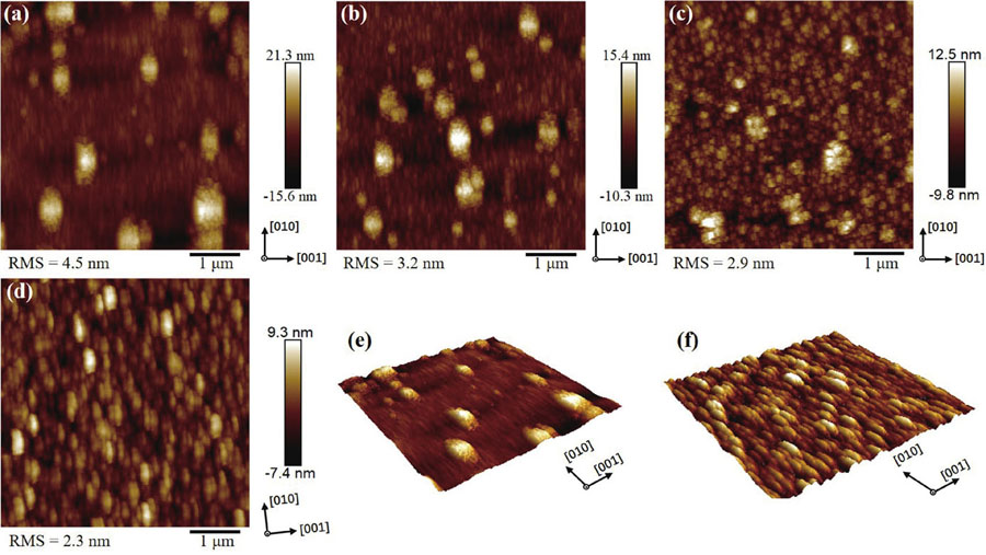
Author Affiliations
Abstract
1 School of Nano-Tech and Nano-Bionics, University of Science and Technology of China, Hefei 230026, China
2 Nanofabrication facility, Suzhou Institute of Nano-Tech and Nano-Bionics, Chinese Academy of Sciences, Suzhou 215123, China
3 Research Center of Laser Crystal, Shanghai Institute of Optics and Fine Mechanics, Chinese Academy of Sciences, Shanghai 201800, China
4 Hangzhou Institute of Optics and Fine Mechanics, Hangzhou 311421, China
Homoepitaxial growth of Si-doped β-Ga2O3 films on semi-insulating (100) β-Ga2O3 substrates by metalorganic chemical vapor deposition (MOCVD) is studied in this work. By appropriately optimizing the growth conditions, an increasing diffusion length of Ga adatoms is realized, suppressing 3D island growth patterns prevalent in (100) β-Ga2O3 films and optimizing the surface morphology with [010] oriented stripe features. The slightly Si-doped β-Ga2O3 film shows smooth and flat surface morphology with a root-mean-square roughness of 1.3 nm. Rocking curves of the (400) diffraction peak also demonstrate the high crystal quality of the Si-doped films. According to the capacitance–voltage characteristics, the effective net doping concentrations of the films are 5.41 × 10¹⁵ – 1.74 × 1020 cm−3. Hall measurements demonstrate a high electron mobility value of 51 cm2/(V·s), corresponding to a carrier concentration of 7.19 × 1018 cm−3 and a high activation efficiency of up to 61.5%. Transmission line model (TLM) measurement shows excellent Ohmic contacts and a low specific contact resistance of 1.29 × 10⁻⁴ Ω·cm2 for the Si-doped film, which is comparable to the Si-implanted film with a concentration of 5.0 × 1019 cm−3, confirming the effective Si doing in the MOCVD epitaxy.
homoepitaxial growth MOCVD Si-doping films high activation efficiency Ohmic contacts Journal of Semiconductors
2023, 44(6): 062801
Author Affiliations
Abstract
1 School of Nano Technology and Nano Bionics, University of Science and Technology of China, Hefei 230026, China
2 Nano Fabrication Facility, Suzhou Institute of Nano-Tech and Nano-Bionics, Chinese Academy of Sciences, Suzhou 215123, China
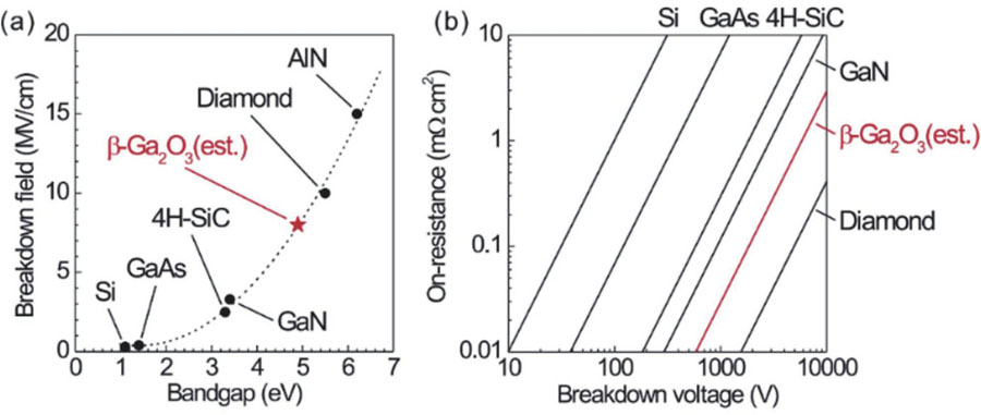
Power electronic devices are of great importance in modern society. After decades of development, Si power devices have approached their material limits with only incremental improvements and large conversion losses. As the demand for electronic components with high efficiency dramatically increasing, new materials are needed for power device fabrication. Beta-phase gallium oxide, an ultra-wide bandgap semiconductor, has been considered as a promising candidate, and various β-Ga2O3 power devices with high breakdown voltages have been demonstrated. However, the realization of enhancement-mode (E-mode) β-Ga2O3 field-effect transistors (FETs) is still challenging, which is a critical problem for a myriad of power electronic applications. Recently, researchers have made some progress on E-mode β-Ga2O3 FETs via various methods, and several novel structures have been fabricated. This article gives a review of the material growth, devices and properties of these E-mode β-Ga2O3 FETs. The key challenges and future directions in E-mode β-Ga2O3 FETs are also discussed.
enhancement mode FETs β-Ga2O3 Journal of Semiconductors
2023, 44(6): 061801
1 中国科学院 苏州纳米技术及纳米仿生研究所加工平台, 江苏 苏州 215123
2 上海科技大学 物质科学与技术学院, 上海 浦东 201210
位姿估计是现阶段智能和自动化控制领域最热门的研究方向之一,在无人驾驶汽车、智能工业机械臂、民用家政机器人等领域有着诸多应用。但传统方法大多具有计算复杂,实时性困难等问题。提出了一种利用卷积神经网络来做双目相机图像输入端的尺寸压缩和信息提取,并将特征向量通过双向长短时神经网络与激光雷达计算的标准结果进行回归学习的位姿解算方案。训练得到的深度学习方案在精度和速度方面相对于传统方案都有一定的提升。
双目相机 位姿计算 深度学习 binocular camera pose computation deep learning
1 桂林电子科技大学 广西精密导航技术与应用重点实验室, 广西 桂林 541004
2 中国科学院苏州纳米技术与纳米仿生研究所 纳米加工平台, 江苏 苏州 215123
3 中国科学技术大学 纳米技术与纳米仿生学院, 合肥 215123
4 南京理工大学 材料科学与工程学院, 南京 210000
提出了一种并联体声波谐振器(BAWR)与Ga2O3基MSM紫外传感器的新型高灵敏度传感器结构, 即体声波谐振式日盲紫外光传感器(BAWR-UV Sensor)。设计并制备了MSM Ga2O3紫外传感器和BAWR传感器, 将实测的光、暗S参数在仿真软件中封装为S1P数据模型代替MSM等效电路, 用MBVD模型代替BAWR等效电路, 通过并联两种结构建立了BAWR-UV仿真模型; 采用ADS软件仿真了BAWR核心参数对BAWR-UV传感器灵敏度的影响, 研究了提高灵敏度的设计方案。仿真结果表明, 在0.5~4.5GHz频率范围内, BAWR-UV的并联Q值越大, 阻抗灵敏度越高, 同时阻抗灵敏度随频率降低而增大, 在并联谐振频率fp=0.533GHz时获得最佳阻抗灵敏度为100kΩ/(μW/mm2); 频率灵敏度随频率的升高而增大, 在fp=4.5GHz时获得最佳频率灵敏度为1.4MHz/(μW/mm2)。最后, 开展了高灵敏度日盲紫外传感器的探索。
日盲紫外探测器 体声波谐振器 氧化镓 叉指传感器 solar blind ultraviolet detector bulk acoustic wave resonator gallium oxide interdigital sensor
1 长春理工大学物理学院,高功率半导体激光国家重点实验室,长春 130022
2 中国科学院苏州纳米技术与纳米仿生研究所纳米加工平台, 苏州 215123
超宽禁带半导体材料金刚石在热导率、载流子迁移率和击穿场强等方面表现出优异的性质,在功率电子学领域具有广阔的应用前景。实现p型和n型导电是制备金刚石半导体器件的基础要求,其中p型金刚石的发展较为成熟,主流的掺杂元素是硼,但在高掺杂时存在空穴迁移率迅速下降的问题;n型金刚石目前主流的掺杂元素是磷,还存在杂质能级深、电离能较大的问题,以及掺杂之后金刚石晶体中的缺陷造成载流子浓度和迁移率都比较低,电阻率难以达到器件的要求。因此制备高质量的p型和n型金刚石成为研究者关注的焦点。本文主要介绍金刚石独特的物理性质,概述化学气相沉积法和离子注入法实现金刚石掺杂的基本原理和参数指标,进而回顾两种方法进行单晶金刚石薄膜p型和n型掺杂的研究进展,系统总结了其面临的问题并对未来方向进行了展望。
金刚石 离子注入 化学气相沉积 超宽禁带半导体 掺杂 n型 p型 diamond ion implantation chemical vapor deposition ultra-wide band gap semiconductor doping n-type p-type
1 长春理工大学, 高功率半导体激光国家重点实验室, 物理学院, 长春 130022
2 中国科学院苏州纳米技术与纳米仿生研究所, 苏州 215123
3 江西省纳米技术研究院, 纳米器件与工艺研究部暨南昌市先进封测重点实验室, 南昌 330200
氮化镓(GaN)高电子迁移率晶体管(high electron mobility transistor, HEMT)以其击穿场强高、导通电阻低、转换效率高等特点引起科研人员的广泛关注并有望应用于电力电子系统中, 但其高功率密度和高频特性给封装技术带来极大挑战。传统硅基电力电子器件封装中寄生电感参数较大, 会引起开关振荡等问题, 使GaN的优良性能难以充分发挥; 另外, 封装的热管理能力决定了功率器件的可靠性, 若不能很好地解决器件的自热效应, 会导致其性能降低, 甚至芯片烧毁。本文在阐释传统封装技术应用于氮化镓功率电子器件时产生的开关震荡和热管理问题基础上, 详细综述了针对以上问题进行的GaN封装技术研究进展, 包括通过优化控制电路、减小电感Lg、提高电阻Rg抑制dv/dt、在栅电极上加入铁氧体磁环、优化PCB布局、提高磁通抵消量等方法解决寄生电感导致的开关振荡、高导热材料金刚石在器件热管理中的应用、器件封装结构改进, 以及其他散热技术等。
氮化镓 功率电子器件 封装技术 高电子迁移率晶体管 开关振荡 散热 金刚石 gallium nitride power electronic device packaging technology high electron mobility transistor switch oscillation heat dissipation diamond

Author Affiliations
Abstract
1 State Key Laboratory on High Power Semiconductor Lasers, Changchun University of Science and Technology, Changchun 130022, China
2 Nanofabrication Facility, Suzhou Institute of Nano-Tech and Nano-Bionics, Chinese Academy of Sciences, Suzhou 215123, China
GaN has been widely used in the fabrication of ultraviolet photodetectors because of its outstanding properties. In this paper, we report a graphene–GaN nanorod heterostructure photodetector with fast photoresponse in the UV range. GaN nanorods were fabricated by a combination mode of dry etching and wet etching. Furthermore, a graphene–GaN nanorod heterostructure ultraviolet detector was fabricated and its photoelectric properties were measured. The device exhibits a fast photoresponse in the UV range. The rising time and falling time of the transient response were 13 and 8 ms, respectively. A high photovoltaic responsivity up to 13.9 A/W and external quantum efficiency up to 479% were realized at the UV range. The specific detectivity D* = 1.44 × 10¹⁰ Jones was obtained at –1 V bias in ambient conditions. The spectral response was measured and the highest response was observed at the 360 nm band.
Journal of Semiconductors
2022, 43(6): 062804


